
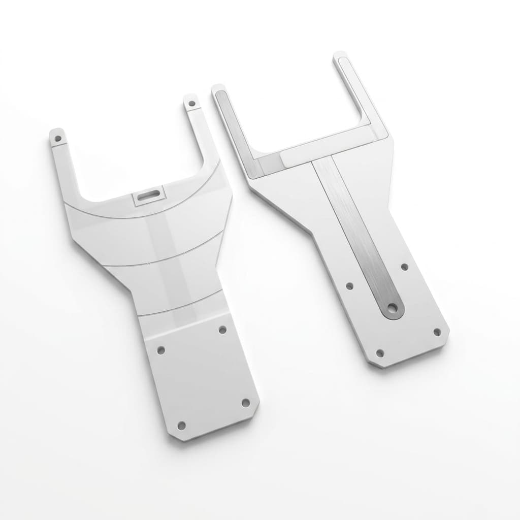
Semiconductor Wafer Handling EOAT Machining: 300mm FOUP Clearances, Cantilever Deflection, and PEEK Blade Tolerances
Specify semiconductor wafer handling EOAT machining: 300mm FOUP clearance budgets, PEEK blade deflection, inspection, and vacuum limits. Request a DFM review.
Semiconductor wafer handling EOAT machining starts with three linked questions: will the blade fit the carrier, will it stay within its loaded motion envelope, and can its contact surfaces meet the process contamination requirements? A drawing that specifies only overall thickness and a polymer trade name leaves all three questions unresolved.
This guide is for automation tooling engineers, Equipment Front End Module (EFEM) integrators, and buyers sourcing CNC-machined wafer blades, vacuum wands, and wrist adapters. Atmospheric EFEM handling and high-vacuum chamber transfer have different retention and contamination constraints; a design approved for one does not automatically qualify for the other.
Quick answer: Start with the actual FOUP and robot interface drawings, allocate the complete insertion envelope, and calculate stiffness before assigning machining tolerances. The 10 mm pitch, 3.30 mm assembly profile, and 0.15 mm deflection allocation discussed below are screening examples, not universal SEMI requirements or proven production capability. A long, uniformly thin PEEK blade may fail the stiffness calculation even when its unloaded geometry fits.
Published and reviewed: November 7, 2026. Scope: Global procurement guidance for nominal 300 mm wafer handling. The numerical examples are reproducible design calculations, not physical test results, customer case studies, or equipment qualification. Thinned, bowed, hot, coated, or bonded wafers require their own payload and clearance inputs. This article does not reproduce licensed standards or approve a robot trajectory.
RFQ shortcut: Send the carrier model, robot interface, STEP model, dimensioned drawing, motion profile, and process environment through Contact / RFQ. For related requirements, see Electronics & Semiconductor Handling EOAT, Vacuum Manifolds & Suction Cup Mounts, Robot Flanges & Adapter Plates, Cleanroom & ESD-Safe EOAT Guide, and Quality Assurance Documentation.
1. Build a 300 mm FOUP Clearance Budget
Treat nominal slot pitch as an input to a stack-up, not as an allowable blade thickness. Obtain the carrier model and revision, shelf profile, door opening, wafer thickness range, bow/warp limits, and robot insertion and lift paths. The SEMI standards portal is the starting point for identifying applicable documents, including SEMI E47.1; confirm the controlled revision and the carrier supplier's interface drawing before release. The portal alone does not substantiate numerical tolerances.
For an illustrative 10.000 mm center-plane pitch with equal 0.775 mm thick wafers, the nominal surface-to-surface opening is 10.000 − 0.775 = 9.225 mm. For unequal wafer thicknesses, subtract half the thickness of each bounding wafer. Shelf intrusions, wafer bow, positional uncertainty, and motion reduce the usable opening further.
Table 1: Illustrative Insertion Budget, Before Picking Up the Wafer
| Budget element | Example value | Interpretation | Release requirement |
|---|---|---|---|
| Center-plane slot pitch | 10.000 mm | Assumed carrier input | Verify carrier drawing and tolerance |
| Bounding wafer thickness | 0.775 mm each | Assumes equal, flat wafers | Use maximum thickness and measured bow |
| Surface-to-surface opening | 9.225 mm | Derived nominal opening | Check shelf geometry over full reach |
| Structural blade core | 2.500 mm | Candidate dimension | Include coatings, covers, and fasteners |
| Contact pad projection | 0.800 mm | Candidate installed height | Include pad tolerance and compression |
| Complete blade profile | 3.300 mm | Core plus pad in this example | Include every protruding feature |
| Upper approach gap | 2.700 mm | Chosen gap below target wafer | Recalculate during approach and lift |
| Lower approach gap | 3.225 mm | Residual gap above lower neighbor | Recalculate for loaded deflection |
| Combined gap reserve | 5.925 mm | 9.225 minus 3.300 mm | Allocate bow, alignment, motion, and uncertainty |
The insertion check closes arithmetically: 2.700 + 3.300 + 3.225 = 9.225 mm. It describes one unloaded approach position. During pickup the blade rises to engage the target wafer, and that wafer then rises off its supports; upper clearance to the next wafer must be checked separately. Do not subtract the target wafer twice or treat an unloaded insertion budget as a loaded-motion approval.
A project might allocate 0.15 mm to elastic tip movement, but that allocation must fit the worst-case clearance stack and be demonstrated on the assembly. Neither this allocation nor the 3.30 mm example establishes a standard maximum blade thickness.
2. Cantilever Deflection: Check the Numbers Before Choosing PEEK
Use the actual unsupported length from the effective clamp to the load location. Overall blade length and wrist-to-wafer-center distance are not interchangeable with this dimension. A forked or tapered blade also differs from a uniform rectangular beam.
For a first-pass, linear elastic cantilever with a point load at its tip:
- Tip movement:
δ = F × L³ / (3 × E × I). - Rectangular section:
I = b × h³ / 12. - Uniform self-weight contribution:
δ_self = w × L⁴ / (8 × E × I), wherewis load per unit length.
Use newtons, metres, pascals, and metres to the fourth power consistently. b is width and h is thickness in the bending direction. For a vertically accelerating assembly, an equivalent point load is F = m × (g + a_z) when upward acceleration is positive. Horizontal acceleration causes different bending or torsion; applying its magnitude as a vertical load is incorrect.
Worked Screening Example: Why an Apparently Thin Blade Can Fail
Assume a uniform blade with L = 0.400 m, b = 0.080 m, h = 0.0025 m, an assumed modulus E = 13 × 10⁹ Pa, and a 0.125 kg tip payload. These are hypothetical inputs; the modulus is not a certified value for every carbon-filled PEEK grade.
The section moment is 0.080 × 0.0025³ / 12 = 1.042 × 10⁻¹⁰ m⁴. Gravity alone gives F = 0.125 × 9.81 = 1.226 N. Substitution gives δ ≈ 0.0193 m = 19.3 mm, before blade self-weight, joint compliance, grooves, or acceleration. That candidate plainly fails an illustrative 0.15 mm allocation. Specifying tighter machining flatness cannot cure inadequate stiffness.
For the same point load and uniform section, increasing reach from 350 to 450 mm multiplies deflection by about 2.13. Increasing thickness from 2.5 to 3.5 mm multiplies it by about 0.364, although the thicker assembly consumes another 1 mm of clearance. Shortening unsupported reach, using a stiffer structural body, or moving thickness to a root outside the insertion envelope may be more effective than tightening dimensional tolerances.
These equations are quasi-static screening tools. They do not predict resonant amplification, settling time, wafer slip, or impact response. Use grade- and direction-specific properties, model the actual pockets and joints, then measure tip displacement and wafer stability on the agreed motion trajectory. A screening failure calls for redesign; a screening pass still requires assembly validation.
3. Material Selection: Separate Structure, Contact, and ESD Functions
A stiff structural blade and a replaceable wafer contact pad need not use the same material. Select the body for stiffness, mass, thermal movement, and process compatibility; select the pad for controlled contact, wear, cleanliness, and electrical behavior. Do not turn generic material-family properties into guaranteed performance of the machined assembly.
Table 2: Wafer Handling Material Decision Matrix
| Material candidate | Structural role | Contact / electrical issue | Evidence required before approval |
|---|---|---|---|
| Unfilled PEEK | Machinable polymer body or inserts where stiffness permits | Usually insulating; creep matters under sustained load | Exact grade properties, contact wear, temperature-dependent stiffness |
| Carbon-fiber-filled PEEK | Candidate for higher stiffness at low mass | Fiber exposure, anisotropy, and resistivity vary by grade | Directional modulus, machined-surface particle and electrical tests |
| Semitron ESd 410C PEI | Static-dissipative inserts or qualified components | PEI is not PEEK; do not substitute annealing or service limits | Manufacturer datasheet plus finished-part qualification |
| PAI, such as Torlon 4203 | Candidate for elevated-temperature precision inserts | Moisture conditioning and grade-specific insulation matter | Supplier processing history, dimensional stability, process compatibility |
| Polyimide, such as Vespel SP-1 | Candidate for thermally demanding pads or supports | Wear and electrical properties depend on grade | Exact grade, bake history, wear and outgassing evidence |
| High-purity alumina | Stiff blade or insert where brittle design is acceptable | Edge damage and insulating behavior require assessment | Ceramic grade, edge inspection, mounting stress and particle tests |
| Aluminum with a qualified finish | Stiff machined structural body | Coating integrity and wafer contact need separate control | Alloy and finish certificates, adhesion, cleanliness, grounding checks |
Verified grade distinction: The manufacturer's Semitron ESd 410C datasheet identifies it as polyetherimide and lists an indicative tensile modulus of 5,850 MPa. It distinguishes heat-deflection temperature from continuous service temperature and states that its values are not guaranteed specification limits. Do not use a headline temperature rating or trade name as an assembly design approval.
The EOS/ESD Association standards resources support selecting the applicable ESD control program and test methods. They do not establish a single universal surface-resistivity acceptance window for every wafer end effector. Specify whether the requirement concerns surface resistance, surface resistivity, resistance to ground, charge decay, or wafer charging, together with electrode geometry, humidity, cleaning condition, and test voltage. Carbon-filled PEEK is not automatically qualified as dissipative.
4. CNC Machining DFM and Stress Control for PEEK Blades
Thin polymer blades can move when machining releases residual stress. Agree the manufacturing sequence and inspection state before placing the order; a part held flat on a vacuum chuck may spring away from flat after release.
A practical DFM sequence is to confirm the stock grade and orientation, rough the outline and pockets with balanced material removal, release the blank for stabilization, and finish using a fixture that does not force it into the desired shape. Leave enough stock for finishing after stabilization. For filled polymers, inspect exposed fibers and tool wear as well as dimensional results.
Use the stock supplier's grade- and thickness-specific annealing instructions. A universal 250°C cycle is inappropriate across PEEK, PEI, and PAI, and heating can change dimensions, crystallinity, or surface condition. Record the approved cycle, support arrangement, and before/after measurements when annealing is part of the purchase specification. Interstage resting is a process control to qualify, not a guarantee of final flatness.
Define surface roughness where it serves contact or cleaning performance, including measurement direction and cutoff. A candidate Ra ≤ 0.4 µm callout must be reviewed for the chosen material and geometry; it is neither a universal cleanroom requirement nor proof of low particle generation. Inspect pocket edges, small ports, and fiber-filled surfaces for loose material. A visually smooth face does not establish cleanliness after repeated motion and cleaning.
5. Vacuum Channels, Seals, and Retention Architecture
Distinguish the operating pressure first. Suction holding force depends on pressure difference: F_hold = Δp × A_effective. In a high-vacuum chamber, ordinary atmospheric suction pads cannot provide the same holding force because surrounding pressure is already low. Edge support, mechanical retention, electrostatic handling, or another qualified architecture may be needed. Bernoulli handling also requires a compatible gas environment.
For an atmospheric blade, review the milled groove, closure method, pad ports, seal glands, fittings, and remaining wall thickness as one assembly. A groove dimension alone says little about pressure at the pad: passage length, conductance, pump curve, leaks, and sensor location affect grip establishment and release time.
Specify a leakage test only with the test gas, differential pressure, method, detection limit, fixture, and acceptance rate. A very low helium leak-rate requirement may suit a particular sealed joint, but it is not a universal wafer-blade acceptance criterion. Distinguish leakage from permeation and trapped volumes, and verify pickup/release behavior at the robot's actual vacuum supply.
Before quoting a closed-channel blade, use Contact / RFQ to identify whether the requirement is an atmospheric suction circuit or a chamber-compatible transport assembly. Include the closure concept and inspection access so the quotation can address manufacturing and qualification work separately.
6. Outgassing and Airborne Molecular Contamination
Particle cleanliness, molecular contamination, and vacuum outgassing are different acceptance topics. A cleanroom air classification does not certify a finished blade, its packaging, or its suitability for an optical or process chamber.
ASTM E595 is a test method for total mass loss (TML) and collected volatile condensable materials (CVCM). The ASTM E595-15(2021) publisher record identifies the referenced edition; access to the full standard may be restricted. Do not describe a test-method citation as a blanket semiconductor certification.
The NASA outgassing database describes testing under ASTM E595 and provides filters for TML, CVCM, water vapor recovered (WVR), and material identity. Its stated application is spaceflight material screening. A database result for one specimen is not approval for every stock form, colorant, coating, adhesive, or finished wafer blade.
If a customer adopts TML ≤ 1.0% and CVCM ≤ 0.1% as screening limits, document them as customer-selected criteria and require matching test conditions and material preparation. Those numbers do not establish compliance with the fab's molecular-contamination limits, process chemistry, or operating temperature. Obtain additional residue, ion, particle, or chamber-recovery evidence where the process owner requires it.
Review every nonmetallic item, including seals and fastener patches. Liquid threadlocker, lubricant, plated hardware, and mechanical locking devices all need process compatibility assessment; none is automatically approved by its category. Vented screws can help evacuate blind trapped volumes, but they do not themselves provide resistance to loosening. Select and qualify locking and venting functions separately.
7. GD&T, Metrology, and PEEK Blade Tolerances
Specify what is measured, how the part is supported, and whether the result concerns a surface or its location. Flatness is a form tolerance and does not reference a datum; pad coplanarity and location relative to the wrist require an appropriate drawing control. A flatness value is the total permitted zone width, not a plus/minus dimension.
Table 3: Inspection Plan to Agree Before Manufacture
| Feature | Drawing decision | Inspection setup | Evidence to request |
|---|---|---|---|
| Wrist mounting face | Flatness zone and surface extent | Support without distorting the face | Measured map and uncertainty |
| Free-state blade form | Zone, orientation, support points | Defined gravity orientation and minimal restraint | Support sketch and surface map |
| Restrained assembly | Functional form and tip location | Wrist simulator, fasteners, torque and sequence | Fixture definition and loaded/unloaded results |
| Contact pad heights | Coplanarity or profile relative to functional datums | Inspect installed pads | Pad-height map with assembly condition |
| Locating bores | Size fit, position, datum system | Inspect bore size and position separately | Bore gauge plus optical/CMM position report |
| Blade thickness and covers | Local profile and minimum remaining wall | Measure specified locations, including closure | Thickness map and joint inspection |
| Contact surface texture | Roughness parameter and sampling direction | Suitable optical or tactile method | Traces, settings, and measurement locations |
For a candidate PEEK blade, 0.050 mm free-state flatness and 0.025 mm restrained flatness can be discussion inputs, not default acceptance limits. Their feasibility depends on reach, cross-section, stock, conditioning, and support. Keep unloaded form, loaded tip displacement, and pad coplanarity as separate requirements so one report cannot substitute for another.
Non-contact metrology can avoid probe-induced bending, but optical measurements still require validation for dark, reflective, or translucent surfaces. Contact inspection can be suitable on supported, stiff features when its influence is quantified. State the method and uncertainty rather than requiring an instrument name as proof of accuracy.
Do not specify an H7 bore without its nominal diameter and governing fit table. Bore size alone does not control position or guarantee tool-center-point repeatability. Inspect the complete locating arrangement and measure replacement repeatability on the robot; re-teaching may still be necessary.
8. 10-Point Engineering and RFQ Procurement Checklist
Use this checklist to turn a concept into a comparable quotation and acceptance plan:
- 1. Interface package: STEP model plus controlled 2D drawing, units, datums, wrist interface, and wafer-facing orientation.
- 2. Carrier identity: Manufacturer, model, revision, shelf geometry, pitch and tolerances; include wafer thickness and bow limits.
- 3. Motion and load: Unsupported reach, wafer mass, acceleration by axis, jerk, settling requirement, and clearance allocation.
- 4. Materials: Exact body and pad grades, stock orientation, traceability, approved substitutions, and temperature range.
- 5. ESD acceptance: Measured quantity, method, environmental conditioning, grounding path, and acceptance range approved by the process owner.
- 6. Retention circuit: Ambient and working pressure, suction or alternative retention method, groove/closure geometry, leakage and response tests.
- 7. Assembly hardware: Fastener material, torque, locking and venting arrangements, seal grade, and approved lubricants or adhesives.
- 8. Inspection: Free-state and restrained setups, form and position controls, uncertainty, sample quantity, and loaded-motion validation.
- 9. Cleaning: Compatible chemistry, rinse, drying and bake procedure, plus particle/residue acceptance and required records.
- 10. Packaging and delivery: Bag material, packing environment, purge if required, identification, handling precautions, and certificates agreed in the order.
Separate prototype machining, special processing, qualification testing, and recurring inspection in the RFQ. Ask suppliers to identify which steps they perform and which require outside services. This makes price and lead-time comparisons meaningful without assuming every quoted blade includes cleanroom processing or vacuum qualification.
9. Frequently Asked Questions
Can a 3.3 mm PEEK blade handle a 300 mm wafer?
Thickness alone cannot answer that question. The 3.3 mm value here includes the pad, while beam stiffness depends on the structural cross-section and unsupported length. The worked example fails gravity-only stiffness despite fitting the nominal insertion opening. Request the actual geometry and load case before accepting a material choice.
Why not use alumina for every wafer handling blade?
Alumina offers high stiffness but requires a design that accounts for brittleness, edge damage, mounting stresses, mass, and electrical behavior. A hybrid structure with replaceable pads may improve serviceability; it still needs process-specific qualification. Neither architecture is universally superior.
Is Bernoulli handling interchangeable with suction pads?
No. Bernoulli handling uses gas flow to create a lifting pressure distribution and usually needs lateral restraint. Assess gas purity, flow, wafer bow, contact exclusions, envelope, and compatibility with the environment. It is not a drop-in solution for a high-vacuum chamber, and it does not guarantee freedom from wafer damage.
Is anodized aluminum prohibited in cleanrooms?
There is no blanket prohibition established by the sources here. Anodize can change electrical behavior and wear performance. The process owner must approve the complete finish, grounding/contact scheme, cleaning response, and particle behavior. Alternative coatings also require qualification rather than automatic acceptance.
Can additive-manufactured PEEK replace machined stock?
Treat it as a new process requiring evidence for porosity, directional stiffness, particle release, cleaning, and outgassing where relevant. A prototype fit check does not approve production wafer contact. CNC machining provides a different manufacturing route, but the finished machined part also needs acceptance testing.
What documentation should arrive with the blades?
Agree the deliverables in the order: material and finish traceability, applicable stabilization records, dimensional reports with fixtures and uncertainty, cleaning and packaging records, and any specified leakage, electrical, or particle-test results. Do not demand a generic certificate that obscures which tests were actually performed.
10. Sources and Engineering Reference Boundaries
- SEMI standards portal — identify applicable carrier/interface standards and obtain controlled revisions. Portal access was restricted during this review; no numerical SEMI clause or tolerance is claimed as verified here.
- ASTM E595-15(2021) publisher record — referenced outgassing test method. The publisher page blocked automated access during review; the test-method description is independently supported by NASA's page. Customer acceptance limits remain separate.
- EOS/ESD Association standards resources — ESD program and test-method resources. The former S20.20-specific URL redirected to this directory; it is not evidence of a universal wafer-tool resistance window.
- NASA Goddard outgassing database — ASTM E595-based material screening records with specimen and preparation context; the former outgassing.nasa.gov address redirects here.
- Mitsubishi Chemical Advanced Materials: Semitron ESd 410C PEI datasheet — grade identity and indicative properties, including their design limitations.
Evidence limits: These references support terminology, material identity, and qualification planning. The clearance allocations, assumed beam inputs, and candidate machining tolerances in this article are explicitly illustrative. No measured blade performance, certified cleanroom capability, or guaranteed fab compatibility is claimed.
11. Request a Wafer Blade DFM Review
For a useful manufacturing review, send the drawing revision, carrier and robot interfaces, body and pad grades, quantity, process environment, and required inspection records. Mark unresolved assumptions, especially stiffness, wafer-contact zones, and closed-channel qualification, so they can be addressed before a production quote.
Use the Contact / RFQ form or email [email protected] to discuss machining feasibility and the processing or testing scope required for your design. Confirm special materials, finishing, cleaning, metrology, and packaging services in the written quotation. Related components include Vacuum Manifolds & Suction Cup Mounts and Robot Flanges & Adapter Plates.
Author

More Posts
Cobot EOAT Machining: Inertia & RFQ Guide
Plan cobot EOAT machining with payload and inertia calculations, contact-edge risk checks, flange tolerances, and an RFQ checklist. Request a CAD/DFM review.

Cleanroom & ESD-Safe EOAT Machining: ISO 14644-1 Procurement Guide
Procurement guide to specify cleanroom and ESD-safe EOAT machining for ISO 14644-1 cells: compare finishes, risks, QA checks, and request DFM support.
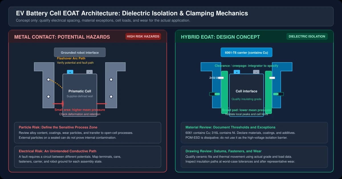
CNC Machining for EV Battery Cell EOAT: Dielectric Isolation, Cu/Zn/Ni Contamination Controls, and Thin-Wall Clamping Mechanics
Specify EV battery cell EOAT machining: dielectric vs ESD materials, Cu/Zn/Ni controls, thin-wall clamp calculations, and an RFQ checklist. Request DFM review.